Ultratechnik.de Pinouts
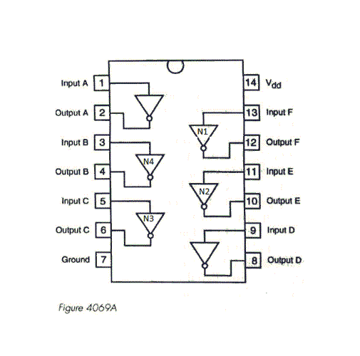
Description CD4069UBMS types consist of six CMOS inverter circuits. These devices are intended for all general-purpose inverter applications where the medium-power TTL-drive and logic-level conversion capabilities of circuits such as the CD4009 and CD4049 Hex Inverter/Buffers are not required.

4069 Hex Inverter Makers Electronics
. TI's CD4069UB is a 6-ch, 3-V to 18-V inverters. Find parameters, ordering and quality information
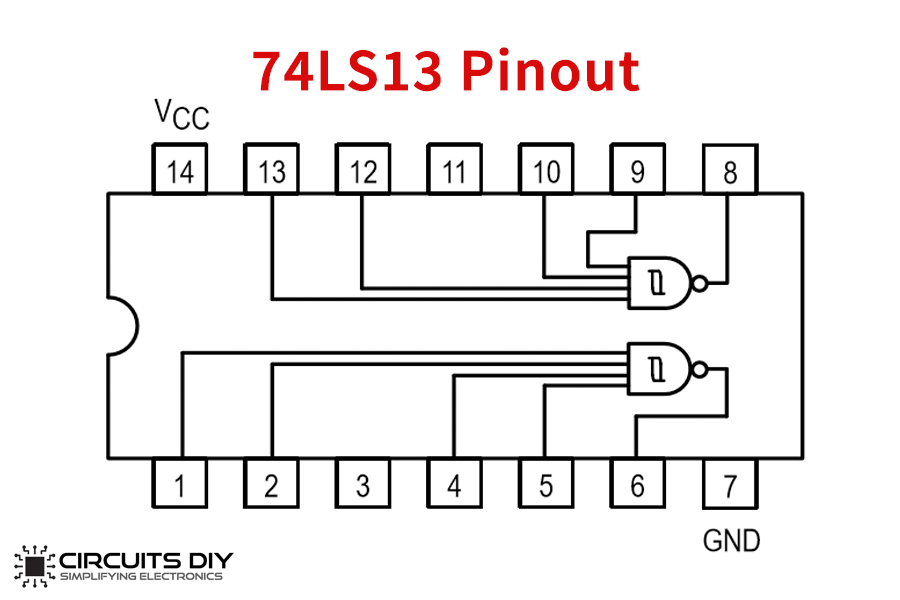
74LS13 Dual 4 Input Schmitt Trigger/ Hex Inverter IC Datasheet
3 Description. The CD4069UB device consist of six CMOS inverter circuits. These devices are intended for all general-purpose inverter applications where the medium-power TTL-drive and logic-level-conversion capabilities of circuits such as the CD4009 and CD4049 hex inverter and buffers are not required.
Asic Pinout Drawer
The CD4069 consists of six inverter circuits and is manufactured using complementary MOS (CMOS) to achieve wide power supply operating range, low power consumption, high noise immunity, and symmetric controlled rise and fall times.

100 Days Free Returns Large online shopping mall 5pcs 10pcs HD63C09EP
The pinout of a 4069UB and 74C14 are identical. Both chips have the same driving capability - about 5 - 10mA per output for a voltage 6v or higher. If you need a larger driving current, use a transistor "buffer" called a Driver Transistor.. THE 4069 The 4069 has an ANALOGUE OUTPUT when configured as an amplifier (as shown above)..

CD4069UB CMOS Hex Inverter
Case Package: PDIP-14. Description: Inverter, CD4069, 6Input, 6.8mA, 3V to 18V, DIP-14. Documentation: CD4069UBE Datasheet (17 Pages) Package Outline Dimension on 4 Page 5 Page 7 Page 8 Page. CD4069UBE User Reference Manual Guide (21 Pages) CD4069UBE Application Note (6 Pages) Pinout Diagram:
Compuerta lógica Inversora CD4069 de Alto Voltaje JaBots
Series. Register once, drag and drop ECAD models into your CAD tool and speed up your design. HEF4069UBT - The HEF4069UB is a hex unbuffered inverter. Inputs include clamp diodes. This enables the use of current limiting resistors to interface inputs to voltages in excess of VDD.
Logic Noise Sawing Away With Analog Waveforms Hackaday
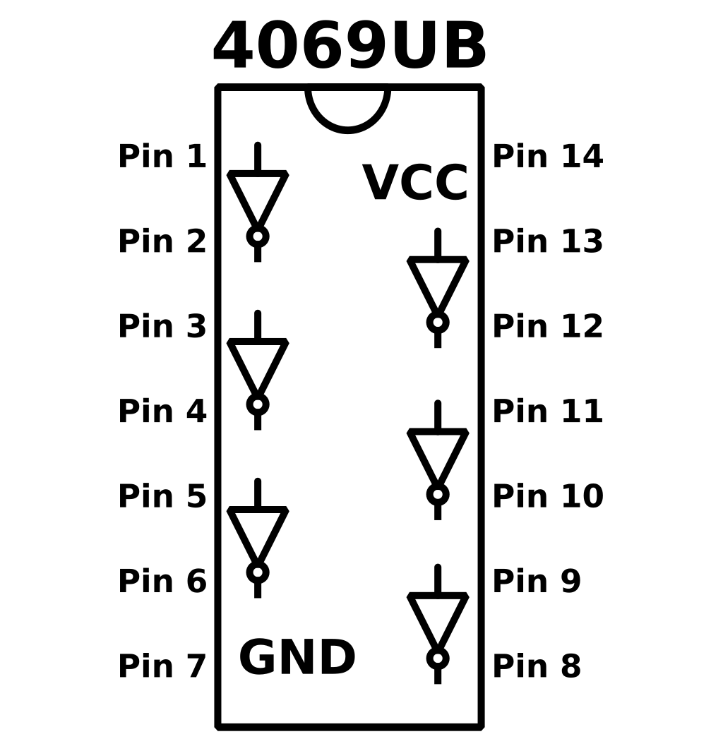
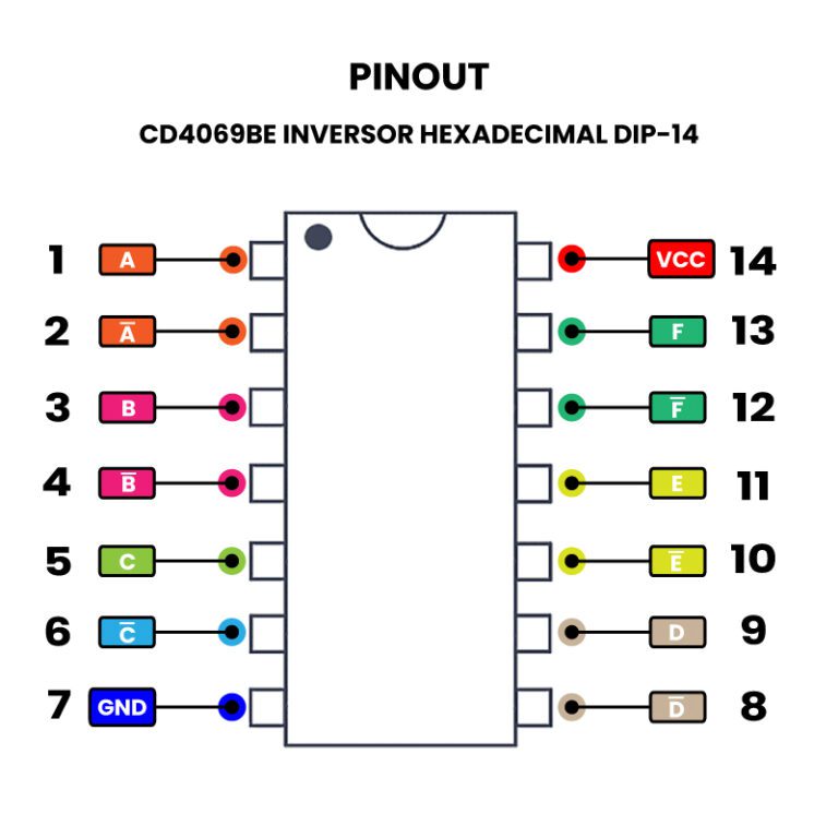
Pin Overview Pin overview for the 4069 IC What is an Inverter/NOT gate? The CD4069 is a CMOS logic chip that contains six independent inverters. It is used to invert a signal, meaning it takes an input signal and produces an output signal that is the opposite of the input. How to Use the CD4069 in a Circuit?
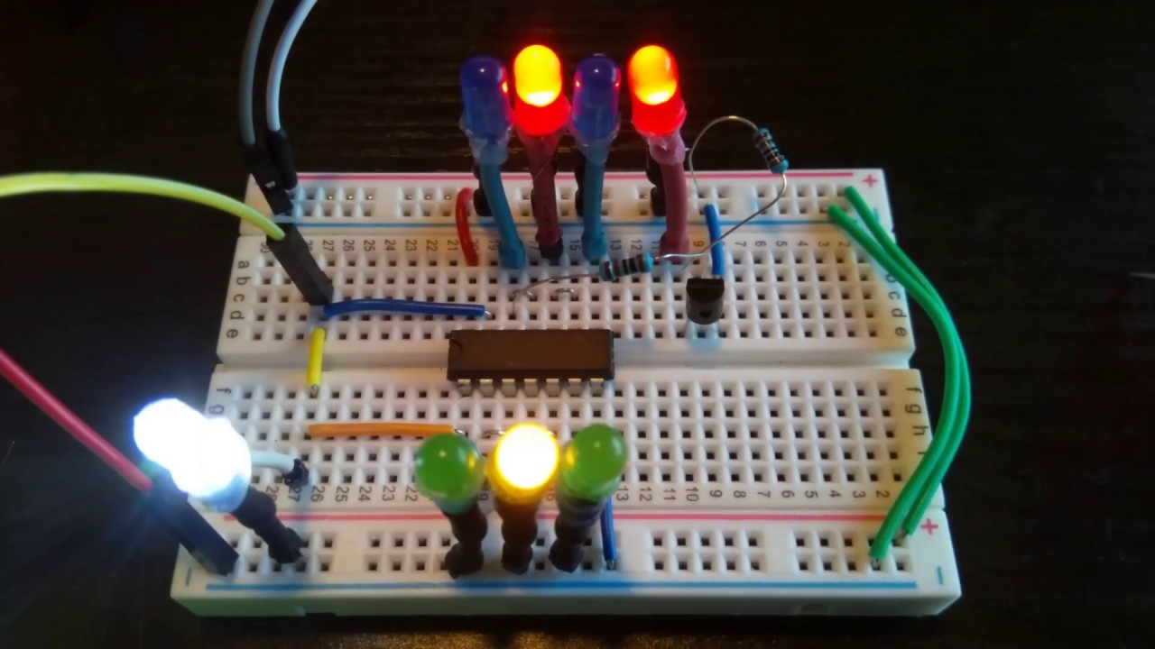
CD4069 HEX inverter YouTube
CD4069UBE - Inverter IC 6 Channel 14-PDIP from Texas Instruments. Pricing and Availability on millions of electronic components from Digi-Key Electronics.
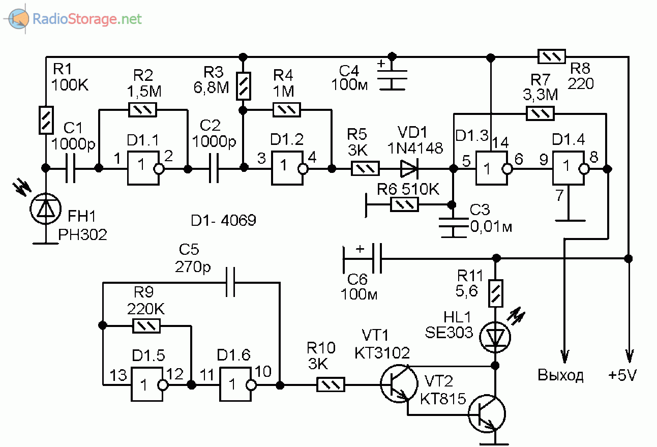
Схемы простых УНЧ, АМрадиоприемника и ИК сигнализации на микросхеме 4069
4069 IC pinout diagram Integrated Circuits Elektropage.com. Loading. Close : Forgot password: Register: Home > Integrated Circuits > 4069. Integrated Circuits ==> LM4781 Lm4734 SST12LP TS27M4C TDA7490L TDA7560 TDA8511J TDA8563AQ TDA8571J TDA8591 TDA7454 TDA7431 TDA7430 TDA7393 TDA7375A TDA7346 TDA7299 TDA7295 TDA7293
UNELESO 2º BCH TI2
Specifications ON Semiconductor CD4069UBCN technical specifications, attributes, parameters and parts with similar specifications to ON Semiconductor CD4069UBCN. Type Parameter Mount Through Hole
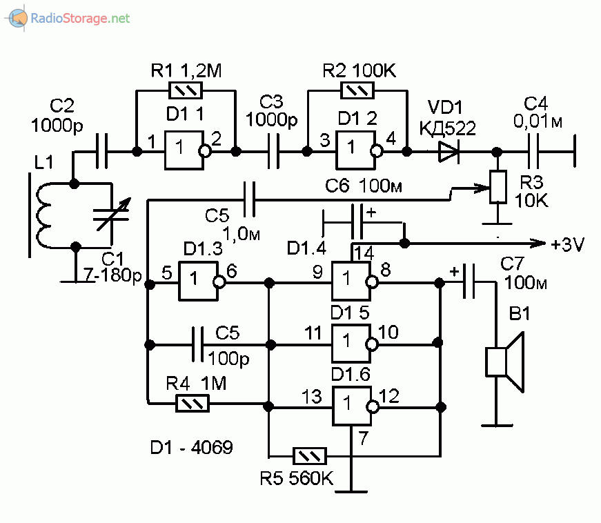
Схемы простых УНЧ, АМрадиоприемника и ИК сигнализации на микросхеме 4069
The IC 4069 is a CMOS hex inverter that contains six independent inverter gates. These are called inverters because these gates will always invert the signal at their inputs to produce an opposite signal at their outputs. Pinout diagram of the IC 4069: Pin 1: Input for inverter 1 Pin 2: Output for inverter 1 Pin 3: Input for inverter 2
CMOS part 2 square wave fuzz PARASIT STUDIO
The CD4069UB consists of six inverter circuits and is manufactured using complementary MOS (CMOS) to achieve wide power supply operating range, low power consumption, high noise immunity, and symmetric controlled rise and fall times.
CD4069BE Inversor Hexadecimal DIP14 UNIT Electronics
MAX485 from Maxim is a low-power transceiver intended for RS-485 and RS-422 applications.It is a half-duplex driver with a Unit Load (UL) rating of 1 and therefore you can have up to 32 MAX485s on a single RS-485 bus. The data rate is up to 2.5 Mbps.MAX485 is available in 8-pin packages of various forms and the typical supply voltage is 5V.
Pickit 3 pinout lasemplaza
CD4069 Pinout. For a detailed description of pinout, dimension features, and specifications download the datasheet of CD4069. Broken Wire Detector Circuit. Working Explanation. IC CD4069 is a device that consists of a six-CMOS inverter with 14 pins that are available in various packages. IC CD4069 is available.
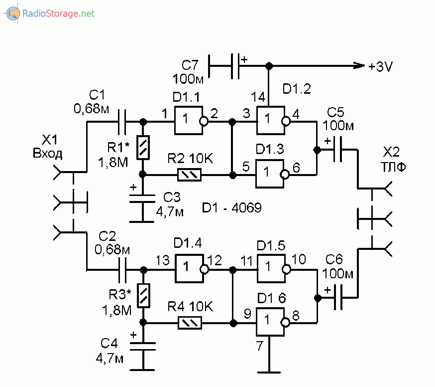
Схемы простых УНЧ, АМрадиоприемника и ИК сигнализации на микросхеме 4069
Applications Example circuits Remember Related Posts Short Description of 4069 See in Fig below. The CD4069 consists of six inverter gate circuits in 14 DIP packets. The manufacturer uses CMOS technology, which allows it to use a wide voltage range of 3V to 16V. Imagine, you are using 2 of 1.5V AA batteries. This IC is working.